Scanning Electron Microscopy Analysis

A powerful analysis technique

Scanning Electron Microscopy Analysis

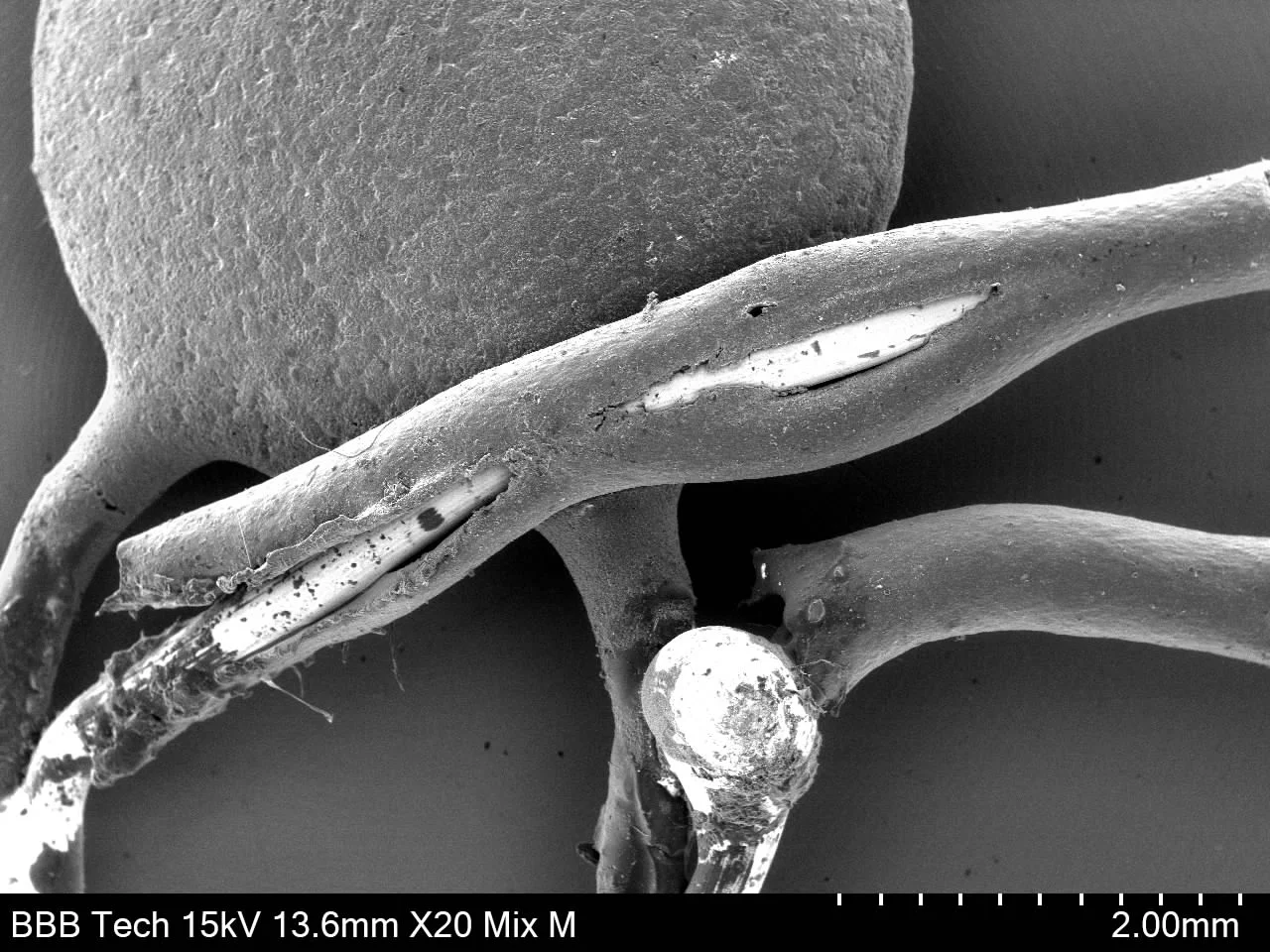
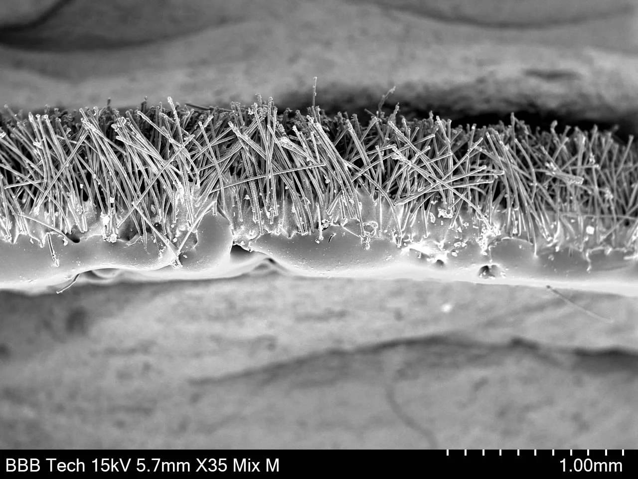
As a leading independent materials testing laboratory, we use a variety of instruments to elucidate the nature of materials. One technique is Scanning Electron Microscopy (SEM), which has emerged as a pivotal tool in materials science, enabling profound insights into the microcosm of various substances. Through the use of focused electron beams, SEM allows our investigators to captures intricate surface details, facilitating a deeper understanding of materials. Its applications span diverse areas, including failure investigation, elemental composition mapping, surface morphology analysis, particle analysis, corrosion studies, and nanotechnology exploration.

In materials analysis, SEM's prowess is evident in its ability to reveal surface textures, grain structures, and mechanical properties. It plays a crucial role in diagnosing failures by examining fracture surfaces and identifying defects. Coupled with energy-dispersive X-ray spectroscopy (EDS), SEM offers a comprehensive view of elemental distributions, assisting in material characterization and quality control.

Metallographic techniques combined with Scanning Electron Microscopy (SEM) analysis offer a powerful synergy that unravels the inner structure of materials. By preparing thin sections or polished surfaces, metallography provides a detailed view of microstructural features such as grain boundaries, phases, and inclusions. When coupled with SEM, these techniques offer enhanced resolution and depth, allowing us to delve into the finest intricacies of materials. This combination enables comprehensive, forensic investigations into material properties, deformation mechanisms, and failure modes, making it an indispensable asset in industries ranging from manufacturing, to aerospace, to simple sealant application.

Utilizing the tandem power of Scanning Electron Microscopy (SEM) and Energy-Dispersive X-ray Spectroscopy (EDS), industries can meticulously analyze contaminants present in their raw materials. The SEM provides high-resolution imaging capabilities that unveil the morphology, distribution, and interaction of contaminants with the material matrix. EDS complements this by identifying the elemental composition of these contaminants with precision. This integrated approach not only aids in identifying the source and type of contaminants but also assists in pinpointing potential sources of material degradation or processing inefficiencies. By harnessing SEM/EDS analysis, industries can ensure the quality and purity of their raw materials, enhance product integrity, and optimise production processes, ultimately leading to improved efficiency and customer satisfaction.

Let our specialists work for you. Contact us today to find out how it can help you. 

Our business is solving problems, so talk to us now.

Contact us