Metallography in electronics.
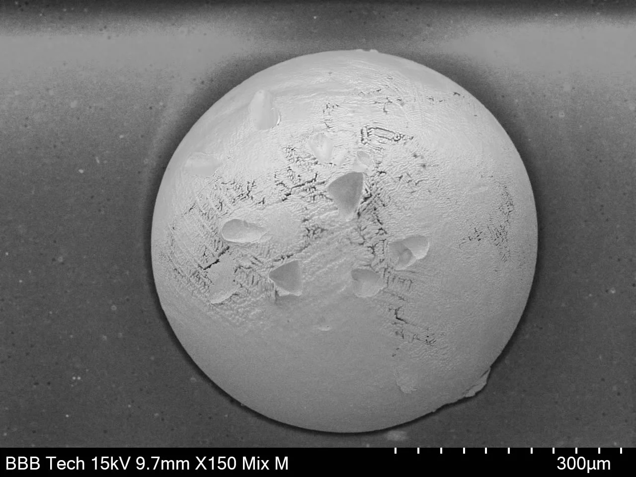
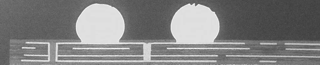
Top-down view of BGA component as received, viewed using scanning electron microscopy.
To enable a more comprehensive examination, the BGA is embedded in epoxy resin, providing stability and preserving its internal structure. This mounting step ensures the delicate features remain intact for further analysis.
Subsequently, metallographic techniques are employed to create a cross-sectional sample of the BGA. Through precise cutting, grinding, and polishing, a flat surface is revealed for scanning electron microscopy (SEM) analysis. This cross-section exposes the internal layers and solder connections, enabling a thorough inspection of potential flaws or irregularities.
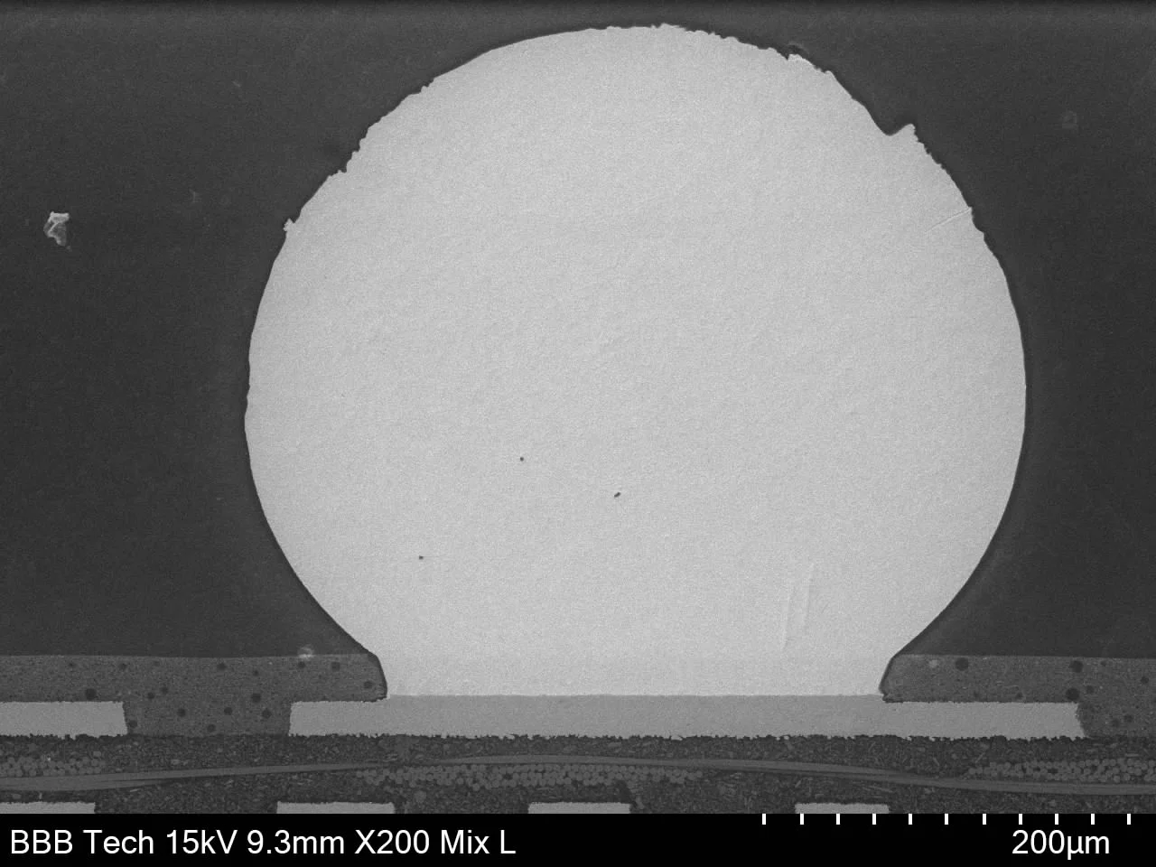
Cross-sectional view of a BGA component, viewed using scanning electron microscopy.
By combining SEM and metallographic techniques, a detailed evaluation of the BGA's internal structure and quality is achieved. This process aids in identifying defects, enhancing reliability assessment, and ensuring the integrity of these essential components in advanced electronics. Contact us today, and get the ball rolling!
Our business is solving problems, so talk to us now.
Contact us